Skip to content

NE555-Internal-Circuit
NE555 - Internal Circuit

We're going a little bit deeper in explaining the NE555.

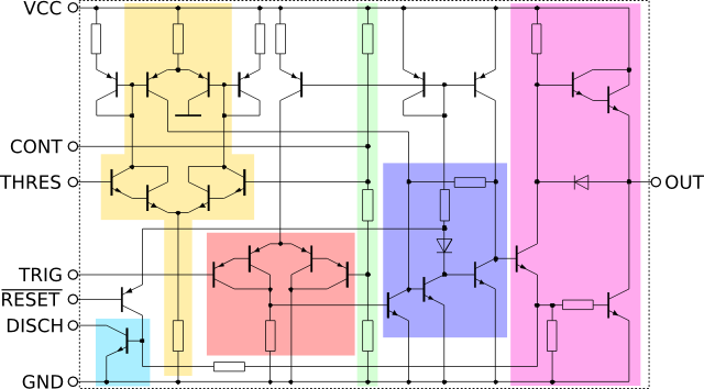
Don't worry about it; nothing difficult will be treated in spite of the complicated picture beside, which could announce a tremendously technical post.

We'll concentrate only on few points to explicate what written in the two previous posts about this IC, especially to see the underlying structure of the S-R latch.

Pins are clearly signed in the electrical scheme representation making easy to recognize them: to facilitate things, inputs 2 and 6 are on the middle-left, power on top-left and bottom-left, and output on the right.
Pin 5 which finally we'll talk about is conveniently going from near 6-threshold to the first node of the triple 5kΩ voltage divider.

...continue reading "NE555 – A deeper look inside"

NE555-Block_Diagram
Block Diagram (wikipedia)

We left last time with some questions about the working core of NE555.
Time to answer.

As we get a digital output from pin 3 (quite Vcc or ground) what about its generation?

We saw the input pins by which we condition the IC, particularly pins 2 (trigger) and 6 (threshold); for now leave pin 5 (voltage control) away.
We will talk about it when we'll have fixed the fundamentals inside our mind.

These two lines go directly to comparators, 2-trigger to the inverting input of the below one while 6-threshold to the non inverting of the above; and as said the comparators give high or low out signal if the voltage input difference is positive or negative respectively.

And finally, outputs to the S-R F-F (Set Reset Flip-Flop).

...continue reading "NE555 – A brief look inside"