As promised last time, let's begin with the idea underlying Serialino's design.
Simply... we wanted to make everyone able to reproduce an Arduino-compatible platform at a reasonable cost, in a quite easy way thanks to the single-sided design, by focusing the communications with pc only on serial port, but without renouncing to an IC for this goal.
The choice of the IC relies upon the classical Max232.
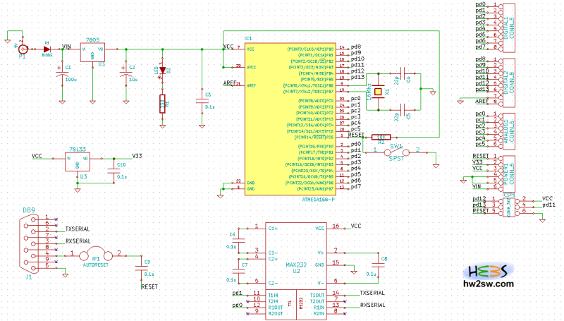
And indeed the ATMega and Max232 are the core of the platform, the biggest components (in DIP format): as well as the ones requiring the major number of connections.
Here is the reason to center them inside the schematic.
Beside them we find the power supplying and external communication parts at left, the input/output headers at right.
A better explanation is needed.
Power Supply Section

We have an external supply input which gives power to the very first important device, the 7805 voltage regulator, to guarantee a constant output voltage of 5V.
[Note that the ATMega 328P requires a maximum input voltage of 5.5V]
The diode protects from an accidental reverse brown-out, while the capacitors have to smooth the signal from undesired interferences.
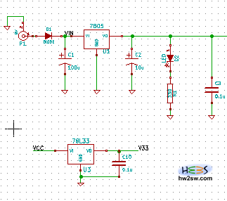
After that, there's a diode with a resistor to show that the board is powered, and again a capacitor to smooth the input signal to the ATMega.
This last one is called Vcc, the power for the micro-controller: the ATMega wouldn't work without it, and as already said it is actually of 5V.
Not only it's the input voltage for the controller, but it becomes an output from one of the 6-pin headers, called POWER_CONN6.
Same for an other source of power, which now is only an output one: in facts a 3.3V signal is given by the second voltage regulator, 78L33.
As the previous regulator's output, it goes to another pin of the same header (where we'll find the ground line on, too).