Ok, we more or less know meaning of Bipolar, Junction and Transistor.
And Common Emitter (or Base or Collector)?
Every electrical circuit wants a voltage reference; as you personally need certainty in life, electrical current is for a voltage one; otherwise it simply doesn't flow.
This reference could potentially be any circuital point at any voltage: for our goals ground (zero voltage) is enough. But this is for the whole circuit
 Common Emitter means that E is used as reference for the other two terminals, whose B is input and C output.
In example schemes you'll usually find (for a NPN BJT) C to the most positive battery, B to the lesser one and E to the ground (eventually with resistors, capacitors and inductors in the middle).
In picture you see and
respectively circuit and polarization power supplies: look at transistor symbol, indicating a NPN with arrow going out from B. PNP has it ingoing, so that NPN has arrow Not Penetrating and PNP has it Penetrating.
As usual resistors limit the amount of current, that could run transistor over leading it to burning.
We've introduced a new term: polarization (or voltage bias). In few words it means the way we put transistor into working condition.
Basically a BJT can be applied as amplifier or switcher (current ON or OFF): in both cases polarization called active sets the transistor to make the current run.
How to do it?
Talking about BJT you must know that on junction zones naturally exists a voltage you can increase or decrease according to your necessities. Its value is around 0.5 or 0.6 V (exceptions excluded).
Well... if you want a NPN BJT active put , so that current can - conventionally - flow from B to E (that is electrons from E to B); you arithmetically add
to
decreasing BE junction voltage and so easing the passage (direct polarization).
On the other side ; this way you make the opposite (note the continuous symmetry!).
is increased so that current cannot go from B to C (or electrons from C to B), but only vice versa (inverse polarization).
With a PNP same talk applies, just with roles inverted.
 Polarization leads transistor to the so called quiescent point or Q-point.
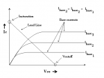
Consider a graph showing the C's current based on , it indicates the current value "actually" flowing through the transistor, being the matching point between current curve and CE resistance's expression.
[Remember Ohm's law: or also
].
R is a line (load line) connecting max voltage to max current, while current's curves depend by B's current for a factor commonly indicated with β, variable from 40 to 400 because of structural features and working temperature .
Picture above shows exactly and quickly what just described.
With one curve set and load line known, Q-point automatically comes out.
This picture shows instead a more common configuration, with a resistance placed between E and ground; equations system returns an interesting result: output gain decreases but stability is guaranteed, while on previous scheme wasn't, so that BJT were possibly exposed to overheating for exceeding current.
[Mathematical explanation is out of our goals, but if you want to know more deeply search for common emitter with degeneration].
