How to read it?
Q is the actual state, whose change (or not) is forced by the S and R inputs.
And this configuration is a latch, so that they are immediately caught by the FF, without the need of an enable (synchronous) signal.
Now suppose that we change S and R to get both of them at 0.
By looking at the two figures of NOR latch circuit and NOR table of truth, you can easily find that the next state will be equal to the actual: we hold the state (of the negated Q too).
This is easy to see by following the lines with their values.
In details we have this situation:
1) the bottom NOR port gets 0 with Q, and the table of truth says to us that it returns Q negated;
2) Q negated goes in input to the top port, again with 0: result is the negation of Q negated, so we get Q next = Q.
Easy to see now that Set (S=1, R=0) and the Reset (S=0, R=1) combinations return Q next equal respectively to 1 and 0.
And now the irregularity we quickly said in the beginning.
What if both S and R are equal to 1?
- the below NOR port has Q and 1; because of the presence of one we surely get output as 0;
- this 0 goes to the above, with another 1, which again forces the result to... 0!
Impossible: we have got Q next = Q next negated!
Or in other words, we just said that 0=1 or vice-versa.
That's why this is called a not allowed state.
So... physically how do we solve this problem?
We simply cannot if the pure S-R latch Flip-Flop is required, and we must wait for the time the IC takes to automatically establish a new stable and allowed state.
If this "instability" is not crucial for the electronic circuit the couple of feedbacks will provide an automatic adjustment in an acceptable amount of time.
[This is possible because the physical device has always asymmetrical behavior that an aseptic table cannot highlight]
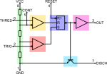
Now let's bind all in the context of the NE555.
We're going to see how the comparators' outputs affect the S-R latch.
Let's begin from the bottom one, with the trigger line (pin 2).
We know that a positive voltage input difference will give High out signal and, as consequence, S=1.
Generally speaking the same behavior for the above comparator, with the difference that output is imposed by the Reset value.

Furthermore note that the trigger and the threshold lines go separately to the inverting and non inverting inputs of comparators, so that the bottom returns High (Low) when trigger is minor (major) than 1/3 Vcc; while the top returns High (Low) when threshold is major (minor) than 2/3 Vcc.
By splitting this two input lines with separated paths we easily avoid the not allowed state, which requires simultaneously trigger < 1/3 Vcc and threshold > 2/3 Vcc.
Just a matter of right management.
Indeed the internal setting brings the trigger line to override the threshold, so that even if the latter is major than 2/3 Vcc, just when the former becomes minor than 1/3 Vcc it imposes its command signal to the F-F, in the sense that the F-F in 555 is realized to accept this.
This makes the not allowed state simply not possible to occur!
Bottom and top comparators connect to Set and Reset of the latch, and now it's clear what they do.
Note that the final inverter and the discharge BJT take the complementary output of Flip-Flop, so that - for example - when pin 2 has V < 1/3 Vcc then S=1 and (for the priority it has onto Reset command) puts Q high, and complementary Q (the negated) low.
Now because just this last one goes as input to the final inverter and to BJT's base, we have that pin 3 gives low negated or high signal, and the BJT's collector has high value too because the transistor is electrically open.
Obviously and if possible, R=1 give the opposite result.
For now it suffices.
Thanks and see you on the next article, with a deeper view of 555!