
We left last time with some questions about the working core of NE555.
Time to answer.
As we get a digital output from pin 3 (quite Vcc or ground) what about its generation?
We saw the input pins by which we condition the IC, particularly pins 2 (trigger) and 6 (threshold); for now leave pin 5 (voltage control) away.
We will talk about it when we'll have fixed the fundamentals inside our mind.
These two lines go directly to comparators, 2-trigger to the inverting input of the below one while 6-threshold to the non inverting of the above; and as said the comparators give high or low out signal if the voltage input difference is positive or negative respectively.
And finally, outputs to the S-R F-F (Set Reset Flip-Flop).
We're dealing with a so called logic digital circuit, capable to pass the value present at its input to its output, keeping it stable.
Its simplicity is based on the fact that inputs themselves modify it immediately.
Here below you see one possible block scheme of a S-R F-F.
You must know that this is the most simple F-F available, and it's affected by an irregularity (more after) which in time has pulled engineers to find out new solutions, but not excluding its design; that's why is important to see it, not only for the present purpose.

By talking about digital components you can encounter the word synthesis: in this context it simply means that a block like an S-R F-F has been designed (and realized) by a synthesis of a chosen boolean representation: logical operations known as AND, OR, NAND, NOR etc... are at the base of the digital circuit ports' design.
In figure we have a NOR (Not OR) synthesis.
Let's see what it means proceeding step by step.
With F-F you become familiar to the concept of state, or the condition which a system is set into.
Furthermore, because F-F are used to modify the state of a system they imply the knowledge of the next state (predictability); at this point you need a scheme to know how to bind the next state by the actual one.
The starting step comprises writing the table of truth for the F-F; and it depends by the table of truth of the specific chosen logic synthesis, here the NOR.
With two generic binary values A and B the OR and the NOR tables of truth are the following:
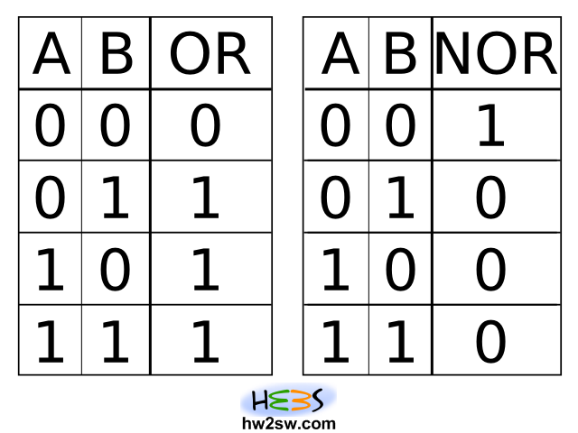
In few words the OR operation takes two operands (here just two, but even more are possible) and returns 1 if at least one of them is 1; otherwise it gives 0.
The NOR, that is Not OR, returns the opposite, because it inverts the results of OR.
Now let's look at how a FF Next-state tables works for the NOR synthesis.
First of all note the outputs signed as Q and Q with a segment on, in the SR NOR Latch figure above: they respectively are the direct out signal and its negated, so the FF returns a couple of complementary signals.