We're going a little bit deeper in explaining the NE555.
Don't worry about it; nothing difficult will be treated in spite of the complicated picture beside, which could announce a tremendously technical post.
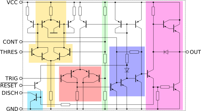
We'll concentrate only on few points to explicate what written in the two previous posts about this IC, especially to see the underlying structure of the S-R latch.
Pins are clearly signed in the electrical scheme representation making easy to recognize them: to facilitate things, inputs 2 and 6 are on the middle-left, power on top-left and bottom-left, and output on the right.
Pin 5 which finally we'll talk about is conveniently going from near 6-threshold to the first node of the triple 5kΩ voltage divider.
Remember where do pin 2 and 6 go relatively to their respective comparators?
Just 2-trigger to inverting, and 6-threshold to non inverting.
And yes... those strange components where they go compose the comparators; no worth here to discuss it.
We're especially interested in the latch behavior, by looking at its inner components... and again we're meeting devices (symbol of them indeed) which resemble the one inside comparators.
We're in trap: it's worth to discuss about them.
Those conflicting segments, whose one has an arrow (pointing internally or externally), form the symbol of a BJT.
While it would be much to talk, we just need to say that if the voltage present at the base B is enough then the voltage between collector and emitter drops to near zero (more or less 0.2V), which makes us possible to consider it electrically closed, with the current free to flow from C to E.
We name this configuration as saturation.
On the other side being the base's voltage not enough then the bjt will electrically open the path from C to E, keeping their voltage drop wider (and blocking - ideally - any current).
We name this configuration as interdiction.
That's basically what we actually need for our purposes!

Or better... we have to explain what enough means for the base's voltage, even supposing that a difference must exist between BJTs with the opposite arrows. And this is so indeed.
Quickly: externally pointing arrow stands for the npn BJT, while the internally one for the pnp BJT.
[To fix: NPn -> Non Pointing to base; Pnp -> Pointing to base]
The n and p letters indicate what kind of doping of electrical charges has been made into the starting "neutral" semiconductor: n for more negative charges and p for more positive (indeed for less negative) ones, dividing the semiconductor into 3 poles (emitter, base, collector) determining the verse which the current must be directed to.
Talking about npn the (positive) current goes from collector to emitter, and base must have quite 0.5V more than emitter; reversely the pnp sees current from emitter to collector, with base's voltage at least at 0.5 less than collector's voltage.
They are opposite (or complementary, if you prefer) by structure and by polarization requests too.