For the first part, click here.
![]()
 On horizontal bar look at the icon here shown: click to run PCBnew, the embedded PCB editor which to design the circuit mask on.
Editor starts with a black ground.

 This helps to highlight the design, to start which Netlist reading is the first step (second picture).
A new dialog window will appear: load your saved .net file by clicking on "Browse Netlist Files", choose it and after that click on "Read Current Netlist".
A little sky-blue pattern is now present on the top-left corner of red frame: they are the components.

 We want them more or less on center of red frame,
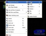
 ![]() and it's possible to move them one by one right-clicking and choosing Move voice from menu as on left picture.
and it's possible to move them one by one right-clicking and choosing Move voice from menu as on left picture.
With a R and a C time spending is reasonable, but for a more general goal is better to learn how to move them all.
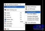
Click on icon as in first right pic, put mouse cursor on center of frame, right-click and choose "Glob Move and Place -> Move All Modules". That's it!
Now move every single footprint in new position around, to clearly distinguish one from the other.


 After footprints positioning it's good to border them with edges.
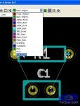
On top horizontal bar click on popup-menu and choose the last voice: "PCB_Edges". This activates mode to make edges.
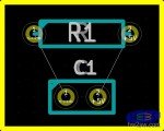
Now go to right, and on icons column click on the one as on second pic (Add graphic line or polygon). Trace the edges and you should get a result like on third pic.
To have references use the grid (you can change its resolution) and the white cross: you'll find them on left icons column, second and sixth respectively.