Schematic job is finished, but it's half work; pcb counterpart and association between them still remain to discover.
Basically pcb presents similar steps to execute, so that every general concept learned until now will result confirmed and will give a whole vision of all.
So first set the correct grid's resolution: we need 50 mils or 1.27 mm or 0.05 inches, and now we can explain this kind of mystery. See following picture.
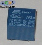
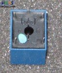
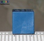
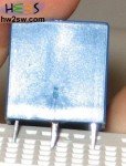 We're learning KiCad to transform software schemes and boards into physical ones; so usually you now which kind of components to use, real components.
Here's the reason: angular pins differ for 5 breadboard holes/steps along the external sides.
The only but important exception is represented by the more external pin, centered so that you can get the right position shifting it at half between two angular ones.
We're underlining this not as style exercise, but to suggest the breadboard use as possible measure when designing for discrete electrical or electronic devices, because pcb's distances and values can reflect the real ones for a 1:1 scale.
Last of above pictures shows what we said: standard steps aren't enough deep, we need half step as resolution.
Note in the second the coil symbol: it indicates the two terminal inductor's pins.
Last but not least, no correlation subsists between EESchema's and PCB's grid values.
 Open PCB and then "Open module editor". Every file related to PCB is a .mod file, that is module.
Set resolution: right-click -> Grid Select -> 50 mils.
Then zoom.


 Now add "New module" and choose a reference name: as always MyRelay rules!
Separate two texts to give a visual order.
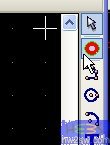
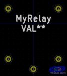

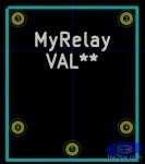 In sequence:
"Add pads";
put pads numbering them as in second picture (right-click -> Edit Pad);
"Add graphic line or polygon";
draw the border, double-clicking to complete it.
Editing numbers respect the logical position represented in the schematics; association requires perfect macth.
I am here repeating that no real correlation exists between schematic and pcb, because first is purely symbolic, useful to represent components - especially in according with international rules -.
Nevertheless give the same pin numbers to a components in all its work spaces.
"Create new library and save current module": dialog window will show directly to kicad's module default directory, where to usually put every module needed for projects.
