We have now enough informations to understand the basics.
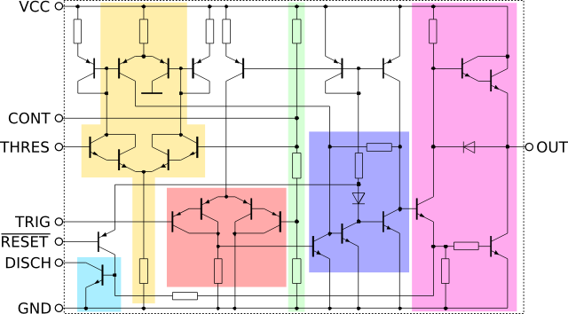
The S-R latch is under the blue/violet colored rectangle.
In order to be clear, name in our minds the three BJTs as Q1, Q2 and Q3 going from left to right.
All they are of npn type.
Well... Q2 and Q3 essentially comprises the Flip-Flop; by following their outputs - here the collectors - you'll easily find them returning back each one into the input of the other, reminding to us the NOR synthesized approach we used to describe the latch.
Q1 provides enough voltage to supply it: in this case being its emitter terminal connected to ground the admitted values are zero (nearly 0.2V) and a bigger voltage, the maximum possible (but alway less than Vcc).
They're good to put the npn in interdiction or saturation (that is electrically closed or open).
Let's see what happens when pin 2 has V < 1/3 Vcc (and pin 6 has V< 2/3 Vcc).
Take as granted the fact that the line (coming from the bottom comparator's output) going to Q1's base has enough voltage to get into saturation: this brings its collector to nearly 0.
But this output becomes the input of Q2 (base), which sees not enough voltage so that it gets into interdiction.
On this hand the Q3's base sees an enough voltage (from Q2's collector voltage) and gets into saturation: its collector's voltage is now zero.
Have you seen what happened?
We entered the latch with an high signal but we exited with a low one: signal has been inverted!
That's because we take the latch's output signal from Q negated (which goes into final inverter).
With this in mind you should have no troubles in finding the reset routing.
Just a last thing about the latch: we said that the trigger line has direct priority onto the threshold, in the sense that even if we took up the reset (S,R)=(0,1) configuration (pin 6 V > 2/3 Vcc), if trigger line gets lower than 1/3 Vcc then we get the potentially not allowed configuration (S,R)=(1,1) but the effects we'll be the same as the Set (S,R)=(1,0): 555's output will be stably high!
The solution key is in Q1, so used non only to start the latch.
In facts by starting from the reset configuration, following the top comparator's output going to Q2's base from top (and to Q1's collector too!), when a valid trigger is captured then it sets all as previously described; in particular Q2's base pass from non-zero to zero voltage.
The result is the output goes from low to high stably!
If you have understood these steps then the routing of signals inside the final inverter won't be a big deal, confirming to you the goodness of what said until now.
And now, what about pin 5?
It affects directly the voltage value on the first node of voltage divider so that it can be externally fixed to a value different from 2/3 Vcc.
Clearly the higher limit cannot overcome Vcc or otherwise we'll get current flowing from that point to positive terminal of power supply. Very bad indeed!
The lower limit simply cannot be less than 1/3 Vcc, for enough trigger's voltage we'll get high comparator's output and again a current flowing from a more positive (in voltage) point to a less positive.
In any case there's no need to this, unless you want to deeply study the IC.
We end with two curiosities.
The first has been introduced in the first post: we asked what could happen when the difference in voltage at a comparator's inputs equals 0.
Intuitively, if a positive difference returns a high signal while a negative just low, we can imagine that a perfectly zero input difference will give a (high - low)/2 voltage.
It's proper to state that sometimes perfection is evil.
The second, maybe one of the first you should have asked yourselves. Why exactly three resistors each of 5k?
Surely from the circuit's designing and dimensioning needs, but according to 555's inventor Hans Camenzind that's because the farm where he worked at the time - Signetics - had “500” numbers, and the earlier product I worked on was the 565, 566 and 567. It was just arbitrarily chosen. It was Art Fury (Marketing Manager) who thought the circuit was gonna sell big who picked the name “555”.
That's all!
Hope you enjoyed our 555 explanation.
More to come on its usage. Thanks!
P.S.: not finished at all. Click HERE to download Camenzind's analog chips designing book in pdf. It's free!